logo
제품 소개Rogers PCB 널

6-Layer Rogers PCB Board with 1.6mm Thickness and 100% Electrical Test for High-Frequency Applications

인증
중국 Bicheng Electronics Technology Co., Ltd 인증
고객 검토
Kevin, Received and tested the boards - thanks very much. These are perfect, exactly what we needed. rgds Rich

—— 부유한 리켓

루스, 나는 오늘 PCB를 얻었고 그들이 단지 완벽합니다. 약간의 인내를 멈추게 하시오 그러면 내 다음 명령은 곧 다가오고 있습니다. 종류는 함부르크로부터 주목합니다 올라프

—— 올라프 쿤홀드

하와이 나탈리. 그것은 완벽했습니다, 내가 참고를 위해 약간의 사진을 첨부합니다. 그리고 나는 예산에 당신에게 다음 2 사업을 보냅니다. 다시 대단히 감사합니다

—— 세바스챤 탑리제크

케빈, 감사, 그들이 완전히 만들어졌고, 잘 작동합니다. 약속된 대로 당신이 나를 위해 제조한 PCB를 사용하는 내 최근의 프로젝트를 위한 링크가 여기 있습니다 : 관계, 다니엘

—— 다니엘 포드

제가 지금 온라인 채팅 해요

6-Layer Rogers PCB Board with 1.6mm Thickness and 100% Electrical Test for High-Frequency Applications

6-Layer Rogers PCB Board with 1.6mm Thickness and 100% Electrical Test for High-Frequency Applications
6-Layer Rogers PCB Board with 1.6mm Thickness and 100% Electrical Test for High-Frequency Applications 6-Layer Rogers PCB Board with 1.6mm Thickness and 100% Electrical Test for High-Frequency Applications

큰 이미지 :  6-Layer Rogers PCB Board with 1.6mm Thickness and 100% Electrical Test for High-Frequency Applications

제품 상세 정보:
원래 장소: 중국
브랜드 이름: Bicheng
인증: UL, ISO9001, IATF16949
모델 번호: BIC-052.V1.0
결제 및 배송 조건:
최소 주문 수량: 1pcs
가격: USD9.99-99.99
포장 세부 사항: 진공 백+상자
배달 시간: 8-9 근무일
지불 조건: t/t
공급 능력: 한 달에 5000pc

6-Layer Rogers PCB Board with 1.6mm Thickness and 100% Electrical Test for High-Frequency Applications

설명
기본 자료: 로저스의 RO4350B 레이어 수: 6 층
PCB 두께: 1.6mm PCB 크기: 110mm × 80mm ± 0.15mm
구리 중량: 내부 및 외부 층 모두에 대해 1oz (1.4 밀) 표면 마감: 전기 니켈 몰입 금 (enig)
강조하다:

6-Layer Rogers PCB Board

,

1.6mm Thickness PCB Board

,

100% Electrical Test RF PCB

Rogers RO4350B 6-Layer PCB: 1.6mm Thickness 100% Electrical Test

This is a 6-layer high-performance PCB constructed with Rogers RO4350B laminate, a woven glass-reinforced hydrocarbon/ceramic composite engineered for high-frequency applications. The PCB integrates advanced material properties with precision manufacturing to deliver exceptional electrical performance, structural stability, and cost-effectiveness for RF and microwave systems.

PCB Specifications
Parameter Technical Details Engineering Significance
Base Material Rogers RO4350B (woven glass reinforced hydrocarbon/ceramic composite) Combines PTFE-like electrical performance with epoxy/glass manufacturability, ideal for high-frequency applications
Layer Count 6-layer rigid configuration Supports complex signal routing with dedicated power/ground planes for EMI control
Board Dimensions 110mm × 80mm ±0.15mm Ensures dimensional stability for automated assembly and enclosure fitting
Minimum Trace/Space 4/4 mils Enables high-density routing with minimal crosstalk in RF circuits
Minimum Hole Size 0.3mm Accommodates fine-pitch components while maintaining structural integrity
Vias 455 total; blind vias (L1-L4, L5-L6); 20μm plating thickness Reduces signal path length and minimizes reflections in high-speed designs
Finished Thickness 1.6mm Provides optimal balance between structural rigidity and weight
Copper Weight 1oz (35μm) for inner and outer layers Ensures low resistance while maintaining high-frequency performance
Surface Finish Electroless Nickel Immersion Gold (ENIG) Delivers excellent corrosion resistance, solderability, and stable RF contact resistance
Silkscreen White on both top and bottom layers Facilitates component identification and assembly verification
Solder Mask Green on both top and bottom layers Protects copper traces while providing environmental resistance
Quality Assurance 100% electrical testing (continuity, isolation, and impedance) Verifies compliance with design specifications prior to deployment
Stack-up Configuration

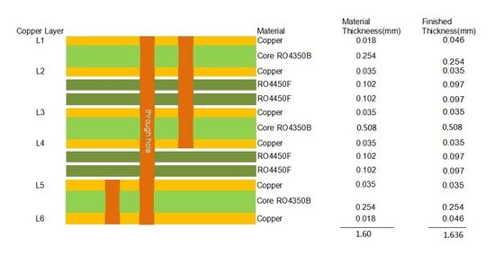
The 6-layer stack-up is engineered for optimal signal integrity and controlled impedance:

Layer Sequence Material/Component Thickness Function
1 Copper Layer 1 35μm Primary signal layer for high-frequency traces
2 Rogers RO4350B Core 0.254mm (10mil) Dielectric layer with controlled Dk for impedance management
3 Copper Layer 2 35μm Ground plane for Layer 1 signals
4 Prepreg RO4450F (x2) 0.2mm Bonding layer with compatible dielectric properties
5 Copper Layer 3 35μm Power distribution layer
6 Rogers RO4350B Core 0.508mm (20mil) Central dielectric providing isolation between planes
7 Copper Layer 4 35μm Secondary ground plane
8 Prepreg RO4450F (x2) 0.2mm Intermediate bonding layer
9 Copper Layer 5 35μm Secondary signal layer
10 Rogers RO4350B Core 0.254mm (10mil) Bottom dielectric layer
11 Copper Layer 6 35μm Auxiliary signal routing layer
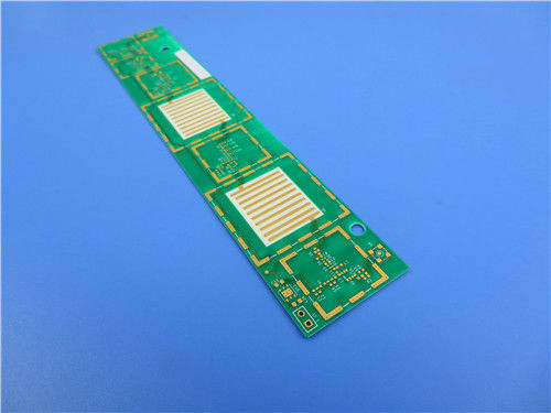
6-layer RO4350B PCB showing detailed board layout and components
RO4350B Material Properties

Rogers RO4350B laminate exhibits key characteristics that enhance PCB performance:

Property Value Technical Impact
Dielectric Constant (Dk) 3.48 ±0.05 @ 10GHz/23°C Ensures consistent signal propagation with minimal variation
Dissipation Factor (Df) 0.0037 @ 10GHz/23°C Minimizes signal loss in high-frequency applications
Thermal Conductivity 0.69 W/m/°K Facilitates efficient heat dissipation from active components
CTE (X/Y/Z) 10/12/32 ppm/°C Matches copper expansion to reduce thermal stress and via fatigue
Glass Transition Temperature (Tg) >280°C Maintains stability during high-temperature processing and operation
Water Absorption 0.06% Prevents performance degradation in humid environments
Flammability Rating UL 94 V-0 Enables use in applications requiring fire safety compliance
Manufacturing and Quality
  • Artwork Format: Gerber RS-274-X, ensuring compatibility with standard PCB fabrication processes
  • Quality Standard: IPC-Class-2 compliance, guaranteeing reliable performance for general electronics applications
  • Processing Compatibility: Compatible with standard FR-4 manufacturing workflows, eliminating the need for specialized processing required by PTFE-based materials
Application-Specific Advantages

The PCB's design and material selection make it particularly suitable for:

  • Cellular Base Stations: Low dielectric loss ensures efficient signal transmission in power amplifiers and antenna systems
  • Automotive Radar: Dimensional stability and thermal performance withstand harsh automotive environments
  • RF Identification Systems: Controlled impedance characteristics support reliable wireless communication
  • Satellite LNBs: Tight Dk tolerance enables precise phase matching in frequency conversion circuits
Close-up view of RO4350B PCB showing surface finish and trace details
Availability

This PCB is available for worldwide shipping, supporting global project requirements.

Conclusion

This 6-layer RO4350B PCB combines advanced material properties with optimized stack-up construction to deliver exceptional performance in high-frequency applications. Its balance of electrical performance, manufacturability, and cost-effectiveness makes it an ideal solution for demanding RF and microwave systems.

Finished RO4350B PCB assembly showing complete board with components

연락처 세부 사항
Bicheng Electronics Technology Co., Ltd

담당자: Ms. Ivy Deng

전화 번호: 86-755-27374946

팩스: 86-755-27374848

회사에 직접 문의 보내기 (0 / 3000)