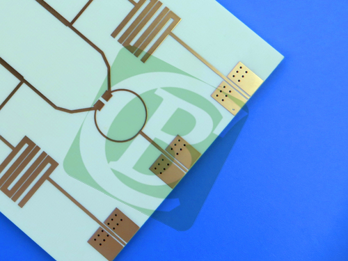
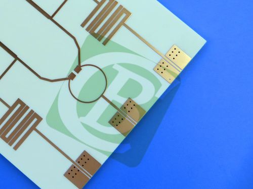
High-Frequency 2-Layer RF PCB RO4730G3 Material ENIG Finish
This is a high-quality, double-sided PCB engineered for radio frequency (RF) applications, particularly suited for antenna systems. It is fabricated using Rogers RO4730G3 antenna-grade laminate, ensuring superior electrical performance, reliability, and cost-effectiveness.
1. PCB Specifications
| Specification Category |
Details |
| Base Material |
Rogers RO4730G3 (hydrocarbon/ceramic laminate) – Low-loss, high-frequency substrate; robust and economical alternative to traditional PTFE-based substrates. |
| Layer Count |
2 layers |
| Physical Dimensions |
- Board size: 59.6mm x 40.5mm (1 piece)- Dimensional tolerance: ±0.15mm |
| Design Rules – Traces & Holes |
- Minimum Trace/Space: 5 mil / 5 mil- Minimum Drill Size: 0.4mm |
| Design Rules – Vias |
- Via Type: Through-hole vias only (no blind vias)- Via Plating Thickness: 20 μm |
| Board Thickness |
Finished board thickness: 0.6 mm |
| Copper Weight |
1 oz (equivalent to 35 μm) on both outer layers |
| Surface Finish |
Electroless Nickel Immersion Gold (ENIG) – Provides a flat, solderable surface with excellent oxidation resistance; optimized for RF performance. |
| Solder Mask |
- Top side: Green (LPI, Liquid Photoimageable) solder mask- Bottom side: No solder mask (exposed copper) |
| Silkscreen |
- Top side: White legend silkscreen- Bottom side: No silkscreen |
2. PCB Stack-up
| Layer Position |
Material |
Thickness |
| Top Layer |
35 μm Copper |
35 μm (1oz) |
| Core Layer |
Rogers RO4730G3 |
0.508mm (20mil) |
| Bottom Layer |
35 μm Copper |
35 μm (1oz) |

3. Key Material Features & Benefits (RO4730G3):
The use of Rogers RO4730G3 material provides significant advantages for RF designs:
-Optimized RF Performance: Stable dielectric constant (Dk) of 3.00 ± 0.05 at 10 GHz and an ultra-low dissipation factor of 0.0028 for reduced insertion loss.
-Low Passive Intermodulation (PIM): Ideal for cellular base station antennas where signal integrity is critical.
-Excellent Thermal Stability: High Tg >280°C and a low Thermal Coefficient of Dk (34 ppm/°C) ensure consistent electrical performance across temperature variations.
-Ease of Fabrication: Fully compatible with standard FR-4 multi-layer processing and lead-free assembly, eliminating the need for specialized PTFE treatments.
-Lightweight & Robust: Unique filler system makes the material 30% lighter than PTFE/glass and features a CTE matched to copper for enhanced reliability.
-Environmental Compliance: RoHS compliant and compatible with lead-free soldering processes.
| Characteristic Category |
Technical Specification |
| Stable Dielectric Constant (Dk) |
3.00 ± 0.05 at 10 GHz |
| Ultra-Low Signal Loss |
Dissipation factor of 0.0028 at 10 GHz |
| Superior Thermal Stability (TCDk) |
Thermal Coefficient of Dk: 34 ppm/°C |
| High Thermal Resilience |
- Glass Transition Temperature (Tg): >280°C- Decomposition Temperature (Td): 411°C (TGA) |
| Controlled Thermal Expansion (CTE) |
- X-axis: 15.9 ppm/°C- Y-axis: 14.4 ppm/°C- Z-axis: 35.2 ppm/°C |
| Efficient Heat Dissipation |
Thermal Conductivity: 0.45 W/mK |
4. Typical Applications:
This PCB is ideally suited for:
-Cellular Base Station Antennas
-Various other RF and antenna applications requiring stable electrical performance and low loss.
Quality & Testing: Manufactured to IPC-Class-2 standards and undergoes 100% electrical testing prior to shipment to ensure functionality and reliability.
Artwork Format: Gerber RS-274-X– the universal industry standard, compatible with fabrication facilities worldwide.
Availability: This PCB is available for order and shipment worldwide.


 귀하의 메시지는 20-3,000 자 사이 여야합니다!
 Korean